1、 The influence of heat conduction and heat dissipation effect
Increasing contact thermal resistance: Poor flatness of the IGBT package bottom and heat sink bonding surface can result in gaps between the contact surfaces, which can increase the contact thermal resistance. The increase in contact thermal resistance will hinder the effective transfer of heat from the IGBT chip to the environment through the heat sink, thereby reducing heat dissipation efficiency.
Impact on heat dissipation performance: The decrease in heat dissipation efficiency can lead to an increase in the operating temperature of IGBT chips, which in turn affects their performance and reliability. High temperature will accelerate the aging process of IGBT and shorten its service life.
2、 The influence of electric field distribution
Although the poor flatness of the bonding surface between the bottom of the IGBT package and the heat sink does not directly cause uneven electric field distribution, the following factors may affect the electric field distribution of the IGBT:
Packaging structure: The packaging structure of IGBT, including packaging materials, packaging processes, etc., may affect the distribution of electric field. For example, impurities, defects in packaging materials, or stress during the packaging process can all lead to uneven distribution of electric fields.
Chip quality: The manufacturing quality of IGBT chips themselves can also affect the distribution of electric fields. For example, the flatness of the chip surface and the lattice structure inside the chip may affect the distribution of the electric field.
3、 Comprehensive impact and solutions
Comprehensive impact: The poor flatness of the bonding surface between the bottom of the IGBT package and the heat sink may affect both thermal conductivity and electric field distribution, thereby affecting the overall performance and reliability of the IGBT. Therefore, in the packaging and heat dissipation design of IGBT, it is necessary to comprehensively consider these factors to ensure the stable operation of IGBT.
Solution:
Improving the flatness of the radiator bonding surface: By improving the processing technology, the flatness of the radiator bonding surface can be improved to reduce the gap between the contact surfaces and lower the contact thermal resistance.
Optimize packaging structure: By optimizing packaging materials, packaging processes, etc., improve the reliability and stability of packaging, and reduce the unevenness of electric field distribution.
Strict quality control: In the production and packaging process of IGBT, strict quality control measures are implemented to ensure product consistency and reliability.
In summary, the poor flatness of the bonding surface between the bottom of the IGBT package and the heat sink mainly affects the heat conduction and heat dissipation effect, rather than directly causing uneven distribution of the electric field. However, this issue still needs to be taken seriously and addressed to ensure the stable operation and long lifespan of IGBTs.
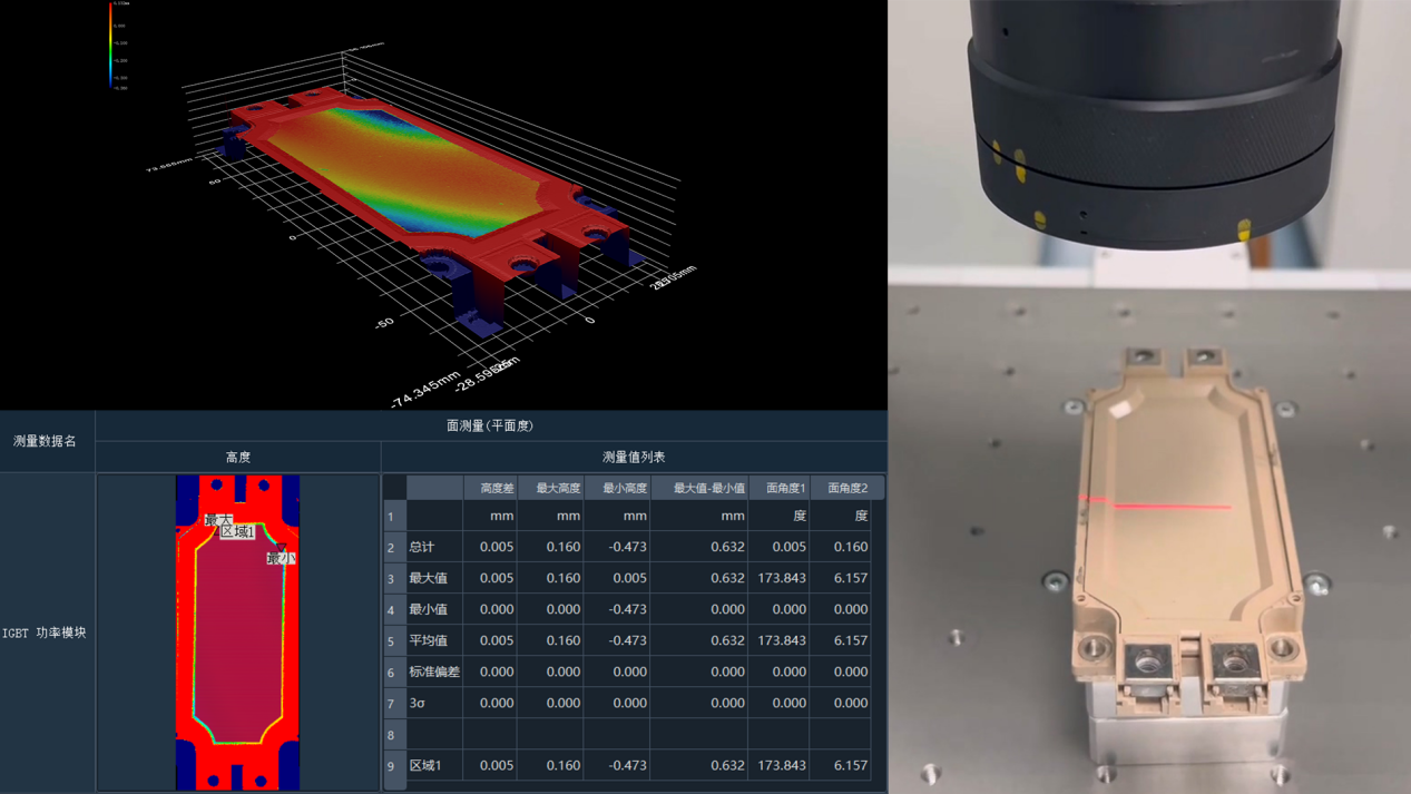
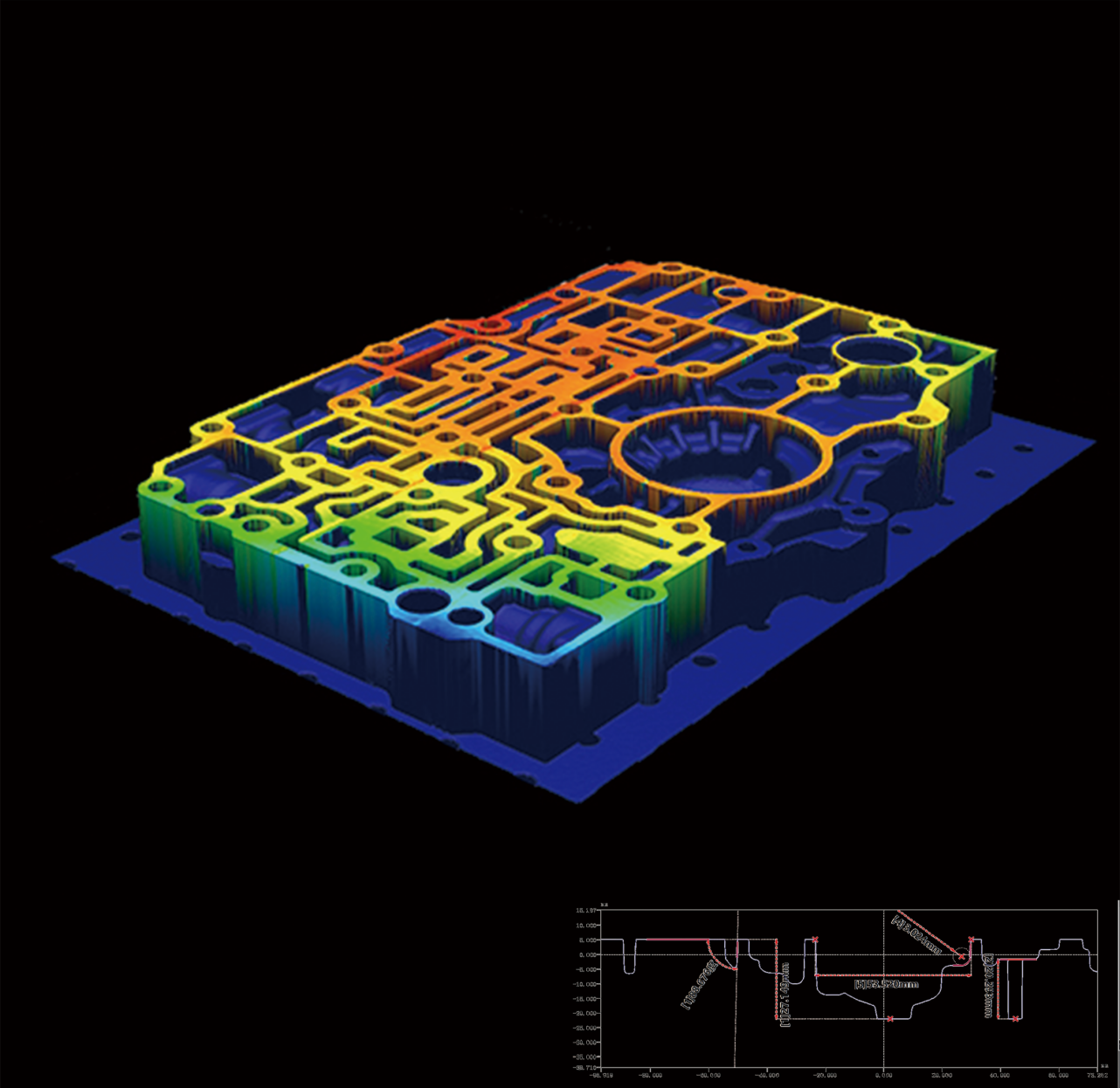
IGBT package bonding flatness test case: (Color temperature chart represents 3D high and low information, table shows measured deformation)
4、 Introduction to Laser Frequency Comb 3D Optical Contour Measurement System
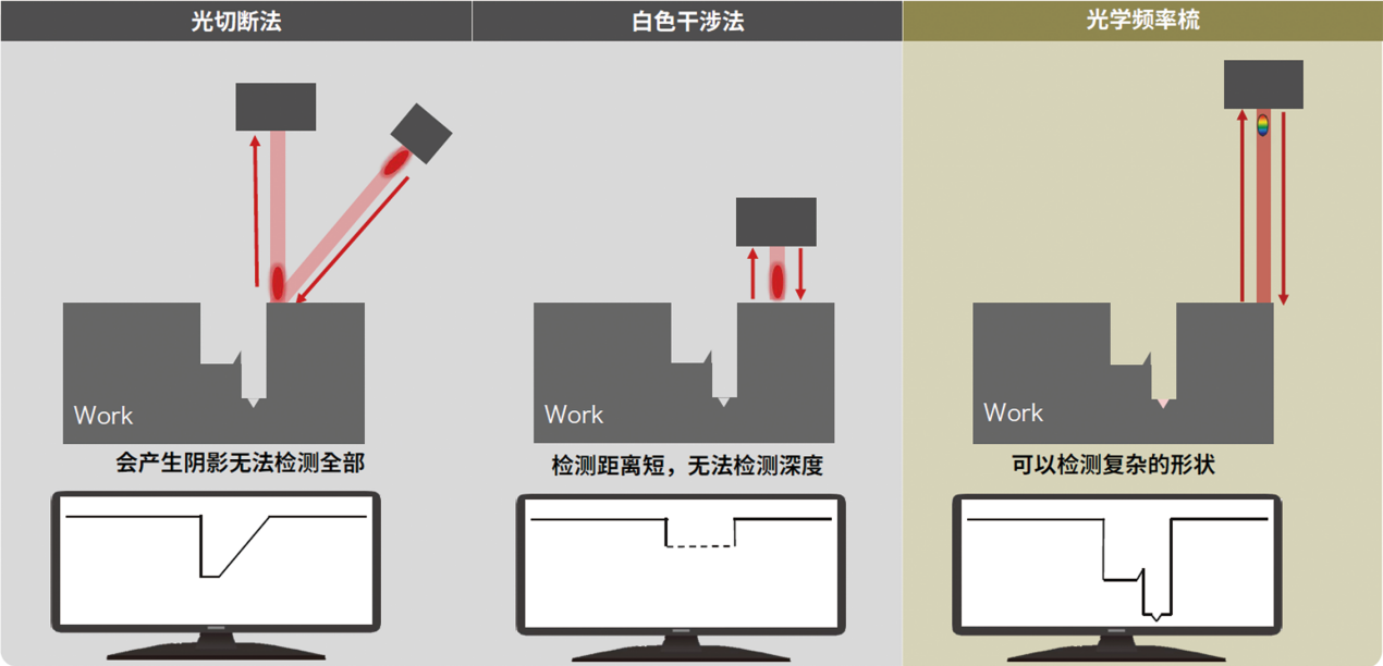
The laser optical frequency comb 3D contour measurement system utilizes the principle of laser frequency comb and adopts high-frequency laser pulse flight distance measurement method, which is not afraid of traditional optical obstruction problems and fully applicable to the measurement of various complex large structural components, solving the difficulties of traditional optical measurement such as deep holes and grooves. The laser frequency of 500kHz has brought technological innovation to the automation of detection.
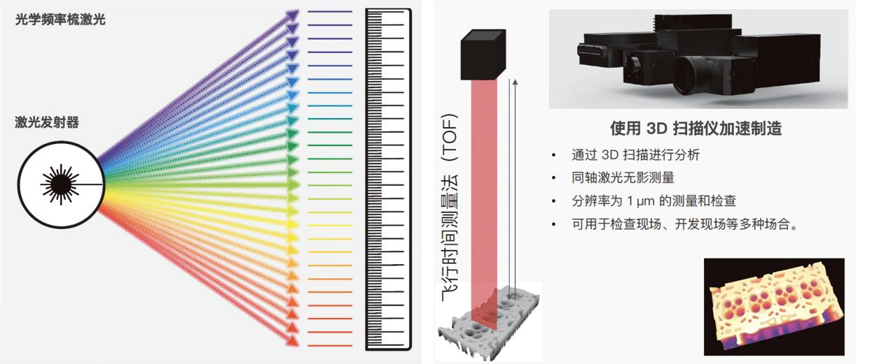
Technical feature one: coaxial shooting, flight ranging scanning method, not afraid of traditional optical "obstruction" problems.
Actual case: Valve body oil circuit board with vertical and horizontal grooves
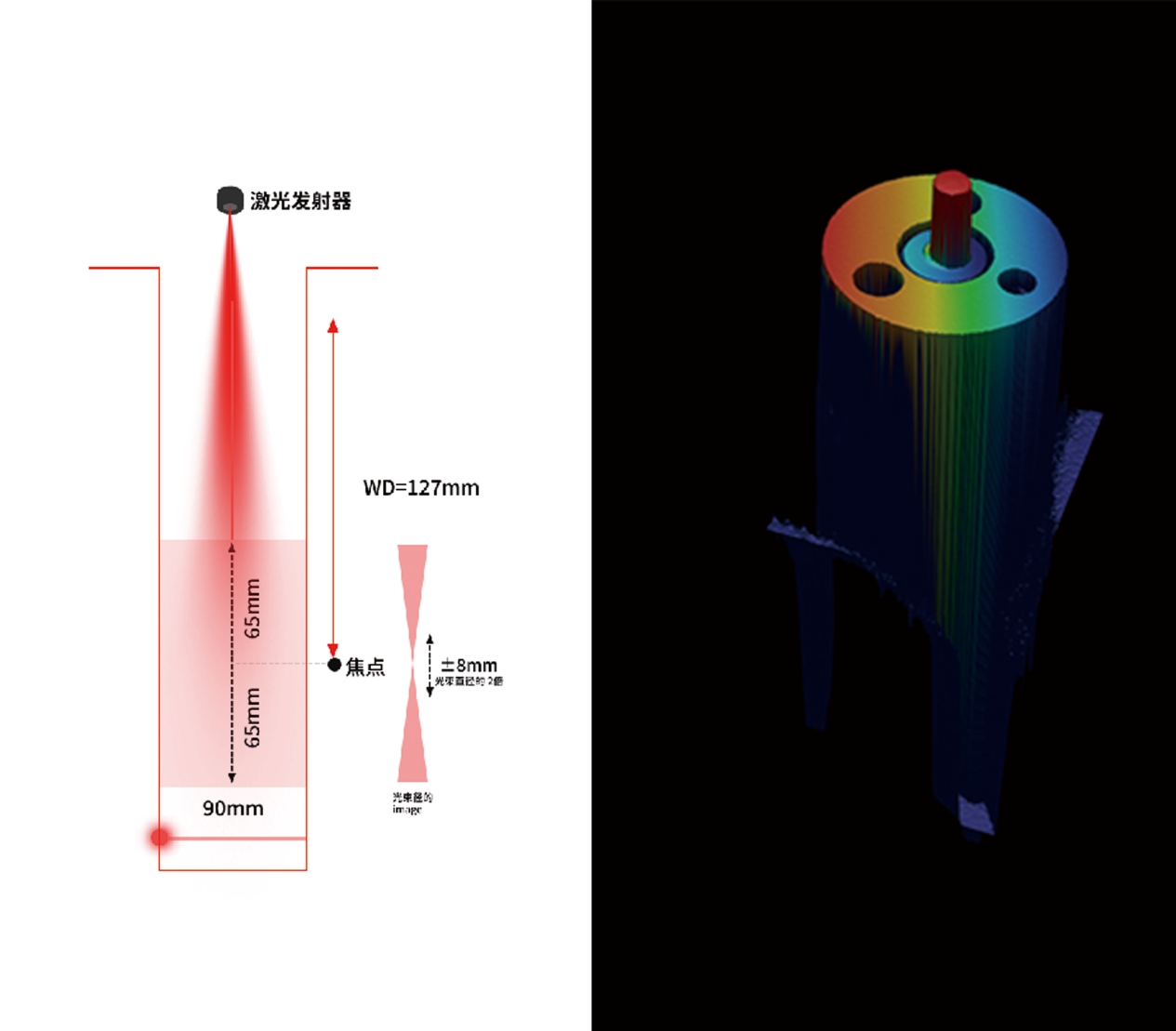
Technical feature 2: With an accuracy of ± 2um, it can achieve a maximum height/depth scanning imaging of 130mm
Technical feature three: It can be equipped with multiple lens combinations to achieve scanning with a large field of view of tens of meters.
