Reduce effective contact area: When the surface flatness of IGBT chips is poor, the contact surface between the chip and the heat sink will no longer be completely adhered. Due to the unevenness of the chip surface, some areas will not be able to form effective contact with the heat sink, resulting in a decrease in the effective contact area. The reduction of effective contact area means that the channel for heat transfer becomes narrower, and the efficiency of heat transfer will be affected.
Increase air gap: The unevenness of the chip surface can also lead to air gaps between the chip and the heat sink. The thermal conductivity of air in these gaps is much lower than that of metals, thus significantly increasing the contact thermal resistance.
2、 The consequences of increased contact thermal resistance
Heat transfer obstruction: The increase in contact thermal resistance leads to the obstruction of heat transfer between the chip and the heat sink. The heat generated by the chip cannot be effectively transferred to the heat sink in a timely manner, which in turn affects the heat dissipation performance of the IGBT.
Temperature rise: Due to the obstruction of heat transfer, the temperature of the chip will rise. High temperature will accelerate the aging process of IGBT and shorten its service life.
Performance degradation: The increase in chip temperature can also lead to a decrease in IGBT performance, such as slower switching speed and increased losses. These performance declines will directly affect the performance of IGBT in circuits.
Reduced reliability: Long term operation at high temperatures can decrease the reliability of IGBTs and increase the risk of their failure.
3、 Correlation analysis
The poor surface flatness of chips is an important reason for the increase in contact thermal resistance. Due to the unevenness of the chip surface, the contact between the chip and the heat sink becomes less tight, resulting in gaps. The poor thermal conductivity of the air in these gaps leads to an increase in contact thermal resistance. Therefore, there is a direct correlation between the surface flatness of the chip and the contact thermal resistance.
4、 Measures to reduce contact thermal resistance
Improving chip flatness: By improving the chip manufacturing process, the flatness of the chip surface can be increased to ensure a tight contact between the chip and the heat sink.
Use thermal conductive medium: Apply thermal conductive medium (such as thermal grease or phase change thermal conductive material) between the chip and the heat sink to fill the gap and reduce contact thermal resistance. The selection of thermal conductive medium should ensure good and stable thermal conductivity.
Optimize heat sink design: Adopt more efficient heat sink design, such as increasing heat dissipation area, optimizing heat dissipation structure, etc., to improve heat dissipation efficiency.
In summary, there is a significant correlation between the increase in contact thermal resistance of IGBT modules and the poor surface flatness of chips. In order to improve the heat dissipation performance and reliability of IGBT, it is necessary to strictly control the flatness of the chip surface and take effective heat dissipation measures.
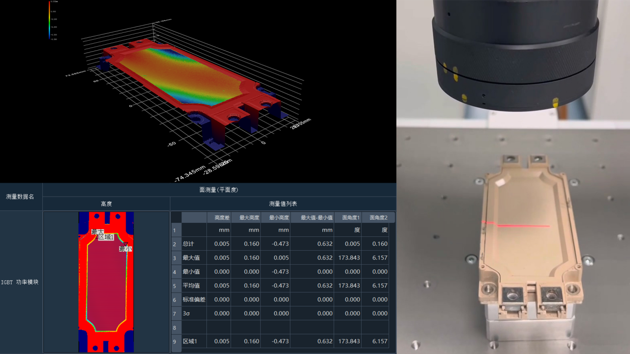
IGBT package bonding flatness test case: (Color temperature chart represents 3D high and low information, table shows measured deformation)
4、 Introduction to Laser Frequency Comb 3D Optical Contour Measurement System
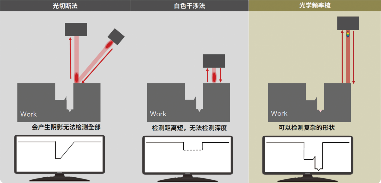
The laser optical frequency comb 3D contour measurement system utilizes the principle of laser frequency comb and adopts high-frequency laser pulse flight distance measurement method, which is not afraid of traditional optical obstruction problems and fully applicable to the measurement of various complex large structural components, solving the difficulties of traditional optical measurement such as deep holes and grooves. The laser frequency of 500kHz has brought technological innovation to the automation of detection.
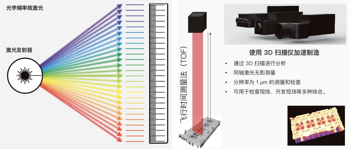
Technical feature one: coaxial shooting, flight ranging scanning method, not afraid of traditional optical "obstruction" problems.
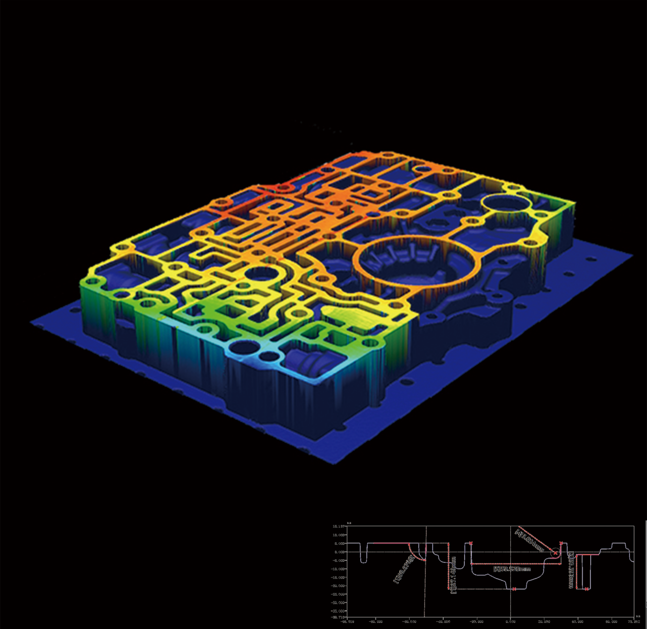
Actual case: Valve body oil circuit board with vertical and horizontal grooves
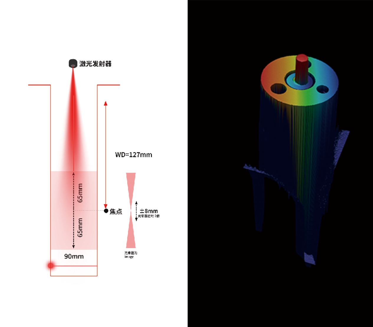
Technical feature 2: With an accuracy of ± 2um, it can achieve a maximum height/depth scanning imaging of 130mm
Technical feature three: It can be equipped with multiple lens combinations to achieve scanning with a large field of view of tens of meters.
