The preparation method of single-sided indium phosphide chips mainly includes the following steps:
1、 Basic preparation process
Grinding: Use grinding solution to grind InP (indium phosphide) chips. Grinding fluid usually contains water, Al2O3 (alumina), and a suspension agent, with Al2O3 particles typically ranging in size from 400 to 600 mesh. The flow rate of the grinding fluid is controlled at 500 to 800 mL/min, and the grinding pressure is 3 to 5 psi.
One time corrosion: Wet chemical corrosion is performed on InP chips to remove abrasive adhering to the surface of the chip and release the stress generated during the processing. Corrosive agents usually contain hydrochloric acid and hydrogen peroxide, and the corrosion time is generally 50-80 seconds.
Thinning: The InP chip is ground with a grinding wheel to further reduce the damage layer, eliminate edge collapse, and improve the flatness of the chip.
Secondary corrosion: Perform wet chemical corrosion on the InP chip again to further remove the stress generated during chip processing. The corrosive agent is the same as a single corrosion, but the corrosion time may be shorter, usually 20-40 seconds.
Rough polishing: Chemical mechanical polishing of InP chips is performed using a polishing pad with a Shore hardness range of 6090 ° and a polishing solution with a chlorine content range of 710g/L. The polishing pressure is 24psi, and the flow rate of the polishing solution is 700900mL/min.
Mid polishing: Chemical mechanical polishing of InP chips is performed using a polishing pad with a Shore hardness range of 2055 ° and a polishing solution with a chlorine content range of 710g/L. The polishing pressure is 1.52.5psi, and the flow rate of the polishing solution is also 700900mL/min.
Precision polishing: Chemical mechanical polishing of InP chips is performed using a polishing pad with a Shore hardness range of 2055 ° and a polishing solution with a chlorine content range of 46.5g/L. The polishing pressure is 1.52.5psi, but the flow rate of the polishing solution is reduced to 300500mL/min.
2、 Other preparation methods
In addition to the detailed preparation steps mentioned above, the preparation of indium phosphide single crystals can also be carried out using the following methods:
Double crucible heating device method: Based on the double crucible heating device, this method effectively reduces the probability of crucible damage during the preparation process of the product, thereby reducing defects such as polycrystals and twinning caused by damage to the inner wall of the crucible during the preparation of indium phosphide single crystals. At the same time, the length of the crystal rod of the obtained product can be significantly increased, and the quality of the crystal can also be improved.
High pressure solution pulling method: Place a quartz crucible containing polycrystalline indium phosphide in a high-pressure equipment, use resistance wire or high-frequency heating, and let the crystal grow under inert gas protection. In order to improve the quality of InP single crystals and reduce dislocation density, doping (such as Sn, S, Zn, Fe, Ga, Sb, etc.) can be used to reduce dislocations.
Gas phase epitaxy method: The disproportionation method of In-PCl3-H2 system is commonly used, in which high-purity indium and phosphorus trichloride react to grow indium phosphide layer.
These methods each have their own characteristics, and suitable preparation methods can be selected according to specific needs and experimental conditions. Meanwhile, strict control of various parameters and conditions is required during the preparation process to ensure the acquisition of high-quality single-sided indium phosphide chips.
5、 High throughput wafer thickness measurement system
The high-throughput wafer thickness measurement system, based on the principle of optical coherence tomography, can solve technical indicators such as wafer/chip thickness TTV (Total Thickness Variation), BOW (Bend), WARP (Warpage), TIR (Total Marked Reading), STIR (Site Total Marked Reading), LTV (Local Thickness Variation), etc.
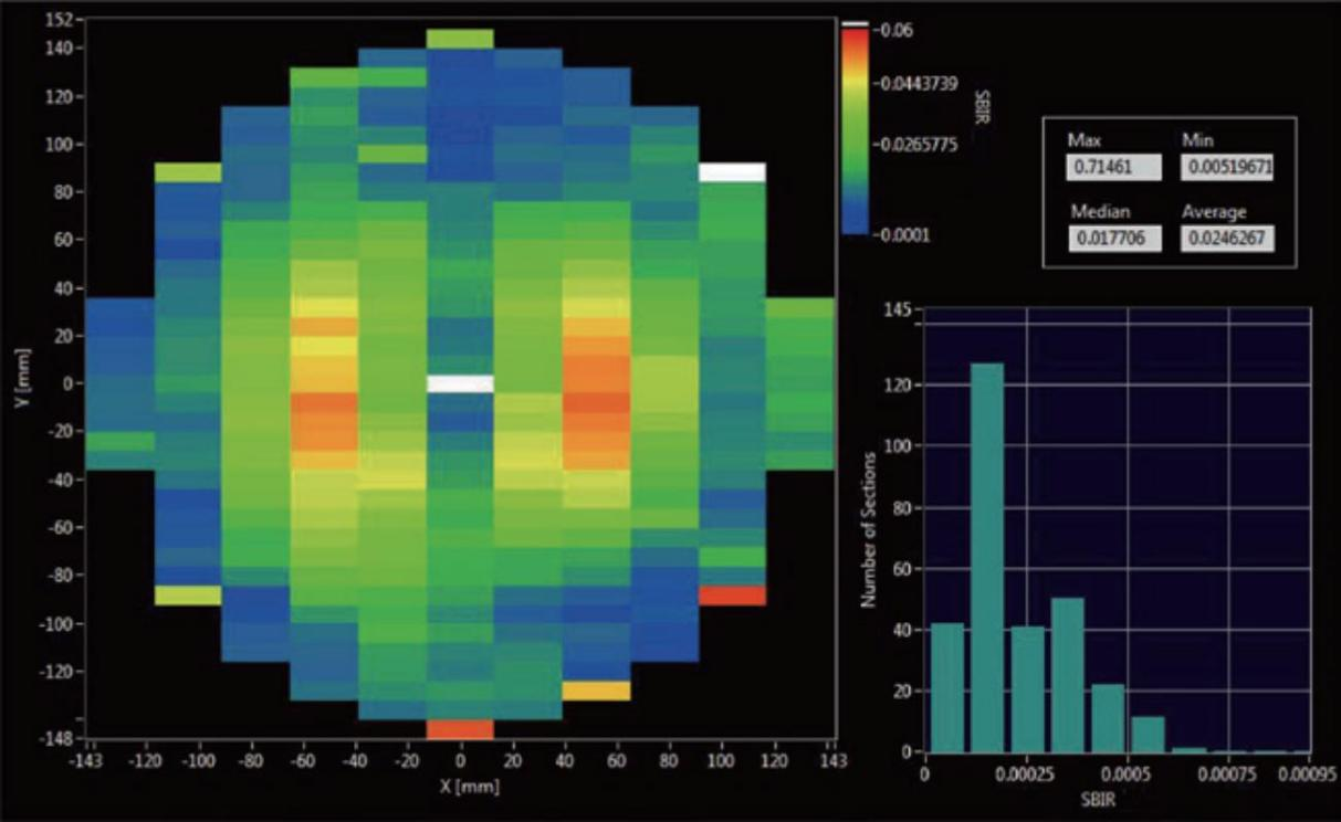
The high-throughput wafer thickness measurement system adopts the third-generation tunable scanning frequency laser technology, which is a traditional dual probe scanning method. It is compatible with 2-inch to 12 inch square and circular wafers, and can measure all flatness and thickness parameters at once.
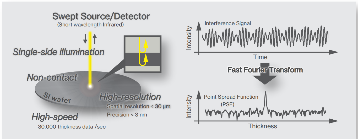
1. Flexible and applicable to more complex materials, from lightly doped to heavily doped P-type silicon (P++), silicon carbide, sapphire, glass, lithium niobate and other wafer materials.

Heavy doped silicon (front and rear surface detection of strongly absorbing wafers)
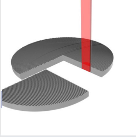
Rough wafer surface, (third-generation scanning frequency laser with point scanning, compared to spectral detection schemes, is less susceptible to interference noise from adjacent units in the spectrum, making it difficult to measure rough surface wafers)
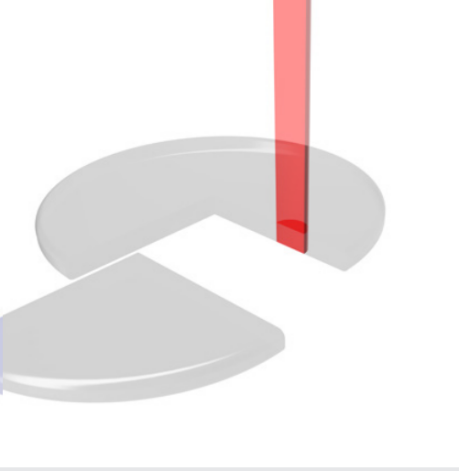
Low reflectivity silicon carbide (SiC) and lithium niobate (LiNbO3); (By compensating for polarization effects, enhance the signal-to-noise ratio of low reflection wafer surface measurements)

Silicon on insulator (SOI) and MEMS can simultaneously measure multi-layer structures, with thicknesses ranging from μ m to several hundred μ m.

It can be used to measure the thickness of various thin films, with the thinnest thickness as low as 4 μ m and an accuracy of up to 1nm.
1. The "temperature drift" processing capability of tunable swept frequency lasers is reflected in their strong anti-interference ability in extreme working environments, which changes the heavy reliance on "active damping platforms" in traditional wafer measurement and significantly reduces costs.
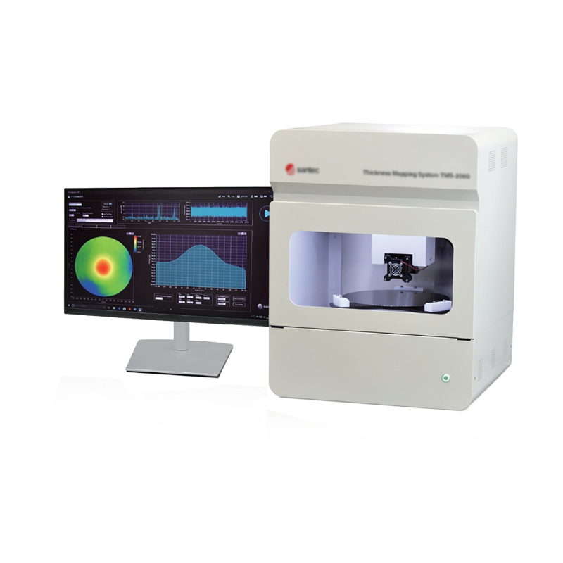
2. Flexible motion control method, compatible with measuring 2-inch to 12 inch square and circular pieces.