The grinding methods for reducing wafer TTV (Total Thickness Variation) mainly include the following:
1、 Adopting advanced grinding technology
Silicon wafer rotary grinding:
Principle: The monocrystalline silicon wafer and cup-shaped diamond grinding wheel adsorbed on the workbench rotate around their respective axes, and the grinding wheel continuously feeds along the axial direction at the same time. The diameter of the grinding wheel is larger than the diameter of the processed silicon wafer, and its circumference passes through the center of the silicon wafer.
Advantages: Single piece grinding, capable of processing large-sized silicon wafers; The grinding force is relatively stable, and active control of the surface shape of single crystal silicon wafers can be achieved by adjusting the inclination angle between the grinding wheel axis and the silicon wafer axis, resulting in good surface shape accuracy.
Double sided grinding:
Principle: Two side symmetrically distributed grippers hold the monocrystalline silicon wafer in the retaining ring, and slowly rotate under the drive of the roller. A pair of cup-shaped diamond grinding wheels are located on opposite sides of the monocrystalline silicon wafer, and are driven by an air bearing electric spindle to rotate in opposite directions and feed along the axial direction to achieve simultaneous double-sided grinding of the monocrystalline silicon wafer.
Advantages: It can effectively remove the waviness and taper on the surface of single crystal silicon wafers after wire cutting, improving grinding efficiency.
2、 Optimize grinding process parameters
By setting reasonable grinding process parameters such as forward pressure, grinding wheel particle size, grinding wheel binder, grinding wheel speed, silicon wafer speed, grinding fluid viscosity and flow rate, wafer TTV can be further reduced. The optimization of these parameters needs to be adjusted according to specific grinding equipment and wafer materials.
3、 Adopting automation and intelligent control
Laser displacement sensor and PLC controller:
Method: Use a laser displacement sensor to measure the flatness of the wafer and transmit the measurement data to the PLC controller. By comparing data and calculating the average value, when the average value of the data is greater than or equal to the preset value, repeat the grinding and processing steps; When the average value of the data is less than the preset value, proceed to the next step.
Advantages: It can quickly measure and calculate flatness, saving frequent manual operations, with fast detection speed, and improving processing efficiency.
Online adjustment technology:
Principle: During the grinding process, the wafer is scanned by a non-contact online measuring device to obtain the thickness deviation TTV value and the specific position of the wafer thickness. Calculate relevant functions based on specific thickness parameters and adjust the angle through an automatic control device.
Advantages: Real time adjustment of grinding parameters can ensure uniformity of wafer thickness and reduce TTV.
4、 Other precautions
Ensure equipment accuracy: The accuracy of grinding equipment has a direct impact on wafer TTV. Therefore, it is necessary to regularly maintain and calibrate the equipment to ensure that its accuracy meets the requirements.
Choosing the appropriate abrasive: The choice of abrasive also has a significant impact on the grinding effect and wafer TTV. Suitable abrasives need to be selected based on the wafer material and grinding requirements.
Control the temperature of grinding fluid: The temperature of grinding fluid has an impact on the grinding effect and wafer surface quality. It is necessary to control the temperature of the grinding fluid within an appropriate range to ensure the grinding effect and wafer surface quality.
In summary, the grinding method for reducing wafer TTV requires starting from multiple aspects such as grinding technology, process parameters, automation and intelligent control, and equipment maintenance. By comprehensively applying these methods, the thickness uniformity of wafers can be significantly improved and the TTV value can be reduced.
5、 High throughput wafer thickness measurement system
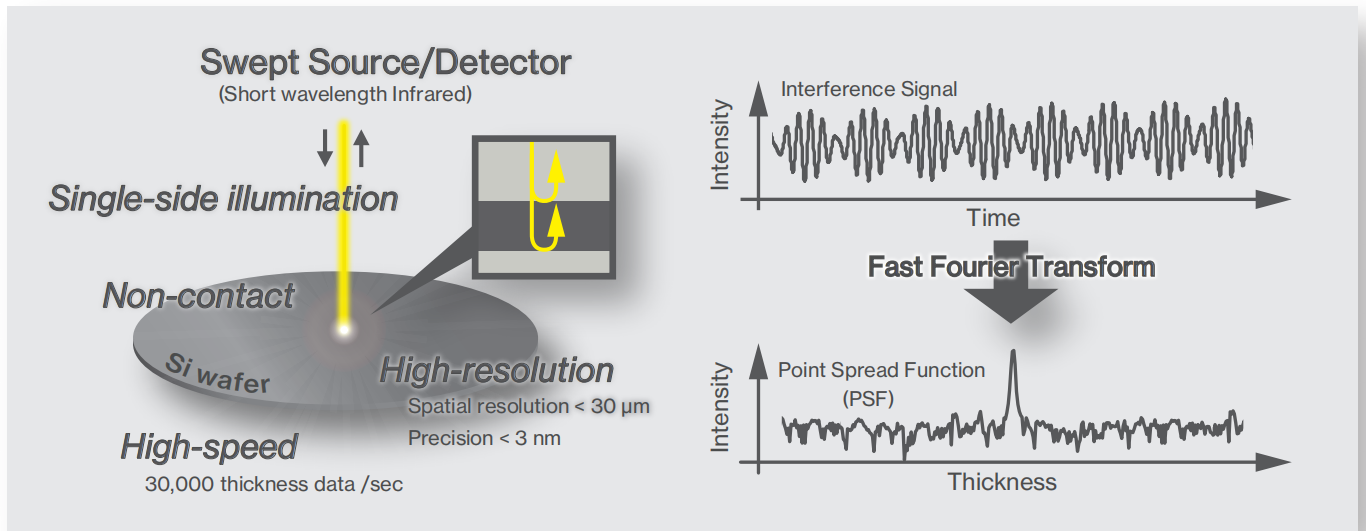
The high-throughput wafer thickness measurement system, based on the principle of optical coherence tomography, can solve technical indicators such as wafer/chip thickness TTV (Total Thickness Variation), BOW (Bend), WARP (Warpage), TIR (Total Marked Reading), STIR (Site Total Marked Reading), LTV (Local Thickness Variation), etc.
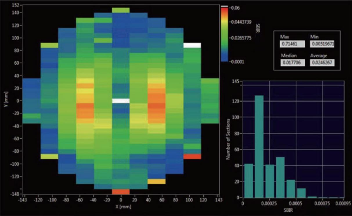
The high-throughput wafer thickness measurement system adopts the third-generation tunable scanning frequency laser technology, which is a traditional dual probe scanning method. It is compatible with 2-inch to 12 inch square and circular wafers, and can measure all flatness and thickness parameters at once.
1. Flexible and applicable to more complex materials, from lightly doped to heavily doped P-type silicon (P++), silicon carbide, sapphire, glass, lithium niobate and other wafer materials.

Heavy doped silicon (front and rear surface detection of strongly absorbing wafers)
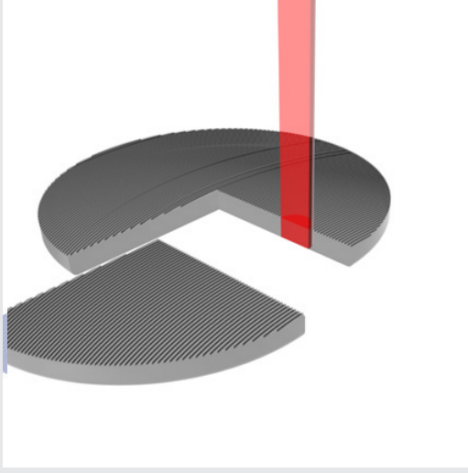
Rough wafer surface, (third-generation scanning frequency laser with point scanning, compared to spectral detection schemes, is less susceptible to interference noise from adjacent units in the spectrum, making it difficult to measure rough surface wafers)
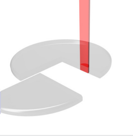
Low reflectivity silicon carbide (SiC) and lithium niobate (LiNbO3); (By compensating for polarization effects, enhance the signal-to-noise ratio of low reflection wafer surface measurements)

Silicon on insulator (SOI) and MEMS can simultaneously measure multi-layer structures, with thicknesses ranging from μ m to several hundred μ m.
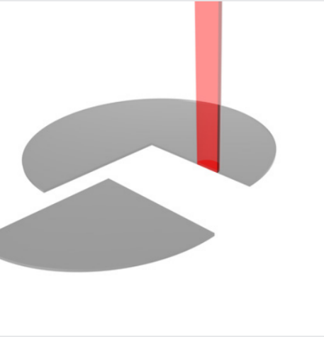
It can be used to measure the thickness of various thin films, with the thinnest thickness as low as 4 μ m and an accuracy of up to 1nm.
1. The "temperature drift" processing capability of tunable swept frequency lasers is reflected in their strong anti-interference ability in extreme working environments, which changes the heavy reliance on "active damping platforms" in traditional wafer measurement and significantly reduces costs.
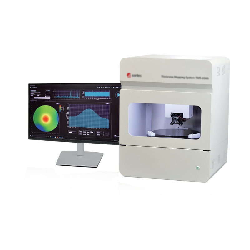
2. Flexible motion control method, compatible with measuring 2-inch to 12 inch square and circular pieces.