The methods for removing edge defects in wafer bonding mainly include the following:
1、 Chemical vapor deposition and planarization process
Method Overview:
Provide wafers to be bonded.
By using chemical vapor deposition, a layer of oxide film with a deposition amount greater than a certain threshold (such as 1.6 TTV) is deposited on the bonding surface of the wafer.
Densification process is applied to oxide thin films.
Flatten the oxide film after densification process to ensure that the grinding amount for planarization and the remaining amount of oxide film meet certain conditions (such as the grinding amount for planarization being greater than 0.9 TTV and the remaining amount of oxide film being greater than 0.4 TTV).
Perform wafer bonding.
advantage:
Through deposition and planarization processes, defects at the bonding edges of wafers can be effectively covered and reduced.
Provide a better substrate for subsequent processes and improve product yield.
2、 Visual inspection and correction technology
Method Overview:
Utilize visual inspection mechanisms to obtain images of the ground wafer.
Obtain the width of edge defects on the wafer based on the image.
Take corresponding measures to treat the edges of the wafer according to the width until the width meets the preset conditions.
Equipment requirements:
The wafer thinning equipment needs to include front-end modules, grinding modules, and control modules.
The grinding module is equipped with a wafer edge processing device and a visual inspection mechanism.
The control module is respectively coupled to the wafer edge processing device and the visual inspection mechanism to implement this method.
advantage:
Visual inspection can accurately obtain the width of wafer edge defects.
Correcting based on the test results can ensure that the defect width at the edge of the wafer meets the preset conditions and improve the quality of the wafer.
3、 Specific process for removing crystal edge defects
Method Overview:
Provide a substrate and form integrated circuit devices on the substrate.
Forming a front-end interconnect structure on a semiconductor substrate.
Form hard mask layer, sacrificial layer and other structures on the front interconnect structure.
Forming sidewall structures through steps such as graphing and etching back, and creating defect sources at the edges of the substrate.
Form a photoresist layer covering the core axis pattern, and use crystal edge etching process to remove the photoresist layer, film layer to be removed, and defect source at the crystal edge.
Remove the remaining photoresist layer and sacrificial layer.
advantage:
This method accurately removes edge defects and avoids the risk of damaging wafer patterns during edge etching processes.
The process is simple, easy to implement, and can improve product yield.
4、 Other precautions
Process selection:
Select appropriate methods for removing bonding edge defects on wafers based on specific wafer materials and process requirements.
Quality Control:
In the process of removing wafer bonding edge defects, it is necessary to strictly control various process parameters to ensure the stability and reliability of the process.
Equipment maintenance:
Regularly maintain and upkeep wafer thinning equipment and related process equipment to ensure their normal operation and accuracy.
In summary, there are various methods for removing edge defects in wafer bonding, including chemical vapor deposition and planarization processes, visual inspection and correction processes, and specific processes for removing edge defects. In practical applications, it is necessary to choose appropriate methods based on specific situations and strictly control process parameters and equipment accuracy to improve the quality and yield of wafers.
5、 High throughput wafer thickness measurement system
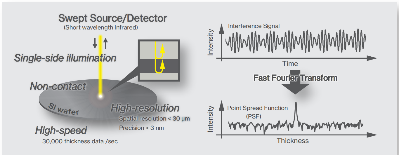
The high-throughput wafer thickness measurement system, based on the principle of optical coherence tomography, can solve technical indicators such as wafer/chip thickness TTV (Total Thickness Variation), BOW (Bend), WARP (Warpage), TIR (Total Marked Reading), STIR (Site Total Marked Reading), LTV (Local Thickness Variation), etc.
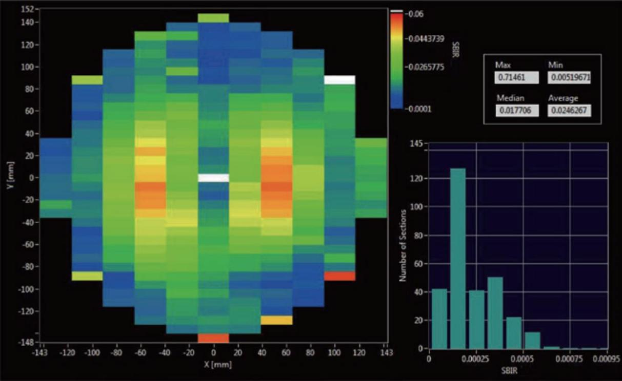
The high-throughput wafer thickness measurement system adopts the third-generation tunable scanning frequency laser technology, which is a traditional dual probe scanning method. It is compatible with 2-inch to 12 inch square and circular wafers, and can measure all flatness and thickness parameters at once.
1. Flexible and applicable to more complex materials, from lightly doped to heavily doped P-type silicon (P++), silicon carbide, sapphire, glass, lithium niobate and other wafer materials.
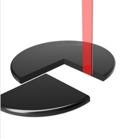
Heavy doped silicon (front and rear surface detection of strongly absorbing wafers)
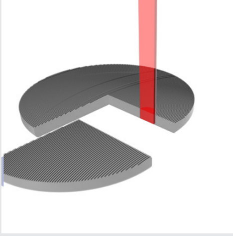
Rough wafer surface, (third-generation scanning frequency laser with point scanning, compared to spectral detection schemes, is less susceptible to interference noise from adjacent units in the spectrum, making it difficult to measure rough surface wafers)
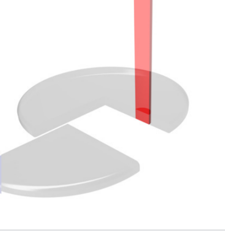
Low reflectivity silicon carbide (SiC) and lithium niobate (LiNbO3); (By compensating for polarization effects, enhance the signal-to-noise ratio of low reflection wafer surface measurements)
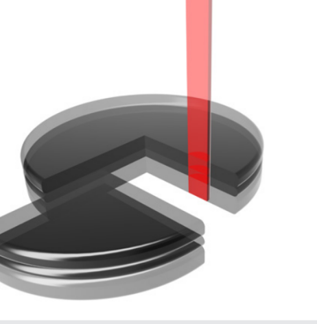
Silicon on insulator (SOI) and MEMS can simultaneously measure multi-layer structures, with thicknesses ranging from μ m to several hundred μ m.
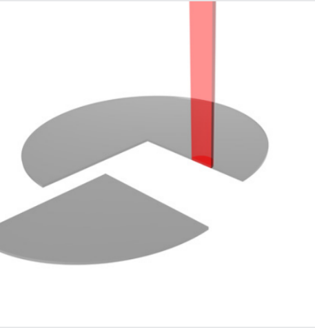
It can be used to measure the thickness of various thin films, with the thinnest thickness as low as 4 μ m and an accuracy of up to 1nm.
1. The "temperature drift" processing capability of tunable swept frequency lasers is reflected in their strong anti-interference ability in extreme working environments, which changes the heavy reliance on "active damping platforms" in traditional wafer measurement and significantly reduces costs.
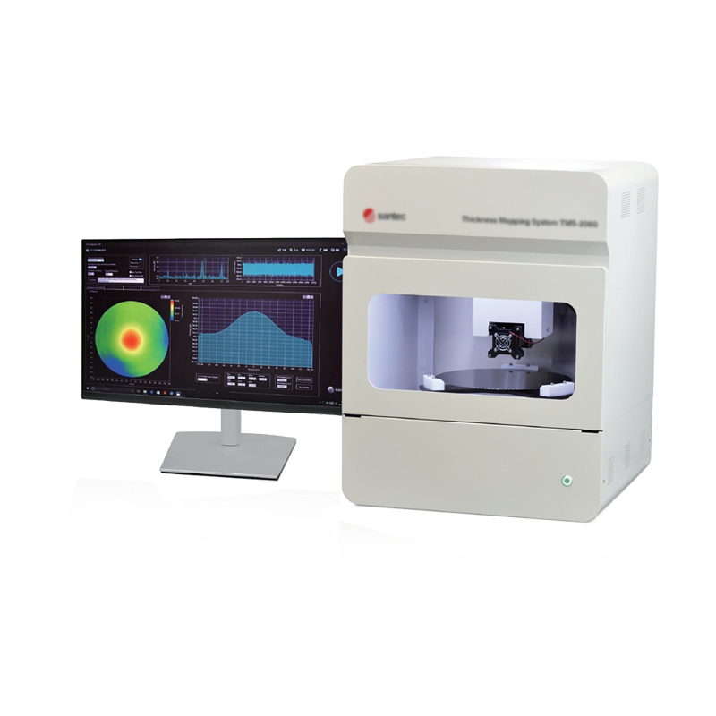
2. Flexible motion control method, compatible with measuring 2-inch to 12 inch square and circular pieces.