The process improvement methods based on quartz glass epitaxial GaN mainly include the following aspects:
1、 Optimization of wafer preparation
Multiple thinning treatments:
By using slurries and grinding discs of different materials to perform multiple thinning treatments on quartz glass, a wafer structure with a predetermined thickness less than 70 μ m and a thickness uniformity TTV of ± 0.5 μ m can be prepared.
This method avoids the risk of mechanical fragility of quartz glass, which can easily lead to the fragmentation of the wafer structure, while ensuring the integrity of the front circuit of the wafer structure.
Polishing treatment:
Polishing the quartz glass after multiple thinning treatments can reduce the surface roughness to below the preset threshold, such as a surface roughness Ra of less than 1nm.
Polishing treatment can significantly increase the density and adhesion of the heat dissipation metal layer electroplating, thereby effectively improving the heat dissipation ability of the wafer structure during operation.
2、 Improvement of epitaxial growth method
MOCVD method:
MOCVD (Metal Organic Chemical Vapor Deposition) is a commonly used epitaxial growth method. By optimizing MOCVD process parameters such as reaction temperature, reactant concentration, and carrier gas flow rate, high-quality epitaxial GaN thin films can be obtained.
The MOCVD method has a high yield and short growth cycle, making it suitable for large-scale production. But after the growth is completed, annealing treatment is required, and the obtained film may have cracks, affecting the product quality.
MBE method:
MBE (molecular beam epitaxy) can achieve GaN growth at lower temperatures, which is beneficial for reducing the volatilization of NH3 in reaction equipment.
However, the growth rate of MBE method is slow and cannot meet the requirements of large-scale commercial production. Meanwhile, when using plasma assisted methods, it is easy to cause damage to the thin film by high-energy ions.
HVPE method:
HVPE (hydride vapor phase epitaxy) has a fast growth rate and produces high-quality GaN crystals. However, high-temperature reactions have relatively high requirements for production equipment, production costs, and technology.
3、 Other auxiliary measures
Substrate selection and processing:
Select appropriate substrate materials, such as Si substrate, and perform appropriate pretreatment, such as cleaning and polishing, to improve the quality and uniformity of epitaxial growth.
Temperature control:
Accurate control of the temperature inside the reaction chamber is crucial during epitaxial growth. Advanced temperature sensors, such as the UV 400 system, can be used to monitor the temperature of the epitaxial wafer surface in real-time, in order to improve the accuracy and stability of temperature control.
Atmosphere control:
Control the atmosphere inside the reaction chamber, such as the partial pressure of NH3 and the flow rate of carrier gas, to optimize the conditions for epitaxial growth.
Subsequent processing:
After the epitaxial growth is completed, the wafer is subjected to subsequent annealing, cleaning, and testing to ensure that its quality and performance meet the requirements.
In summary, the process improvement method based on quartz glass epitaxial GaN involves multiple aspects such as wafer preparation optimization, epitaxial growth method improvement, and other auxiliary measures. By comprehensively applying these methods and technologies, high-quality and high-performance GaN epitaxial wafers can be prepared.
4、 High throughput wafer thickness measurement system
The high-throughput wafer thickness measurement system, based on the principle of optical coherence tomography, can solve technical indicators such as wafer/chip thickness TTV (Total Thickness Variation), BOW (Bend), WARP (Warpage), TIR (Total Marked Reading), STIR (Site Total Marked Reading), LTV (Local Thickness Variation), etc.
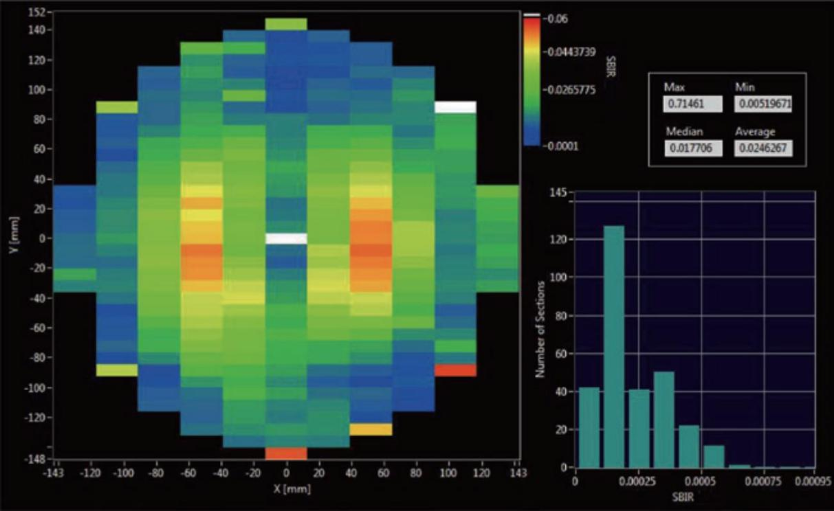
The high-throughput wafer thickness measurement system adopts the third-generation tunable scanning frequency laser technology, which is a traditional dual probe scanning method. It is compatible with 2-inch to 12 inch square and circular wafers, and can measure all flatness and thickness parameters at once.
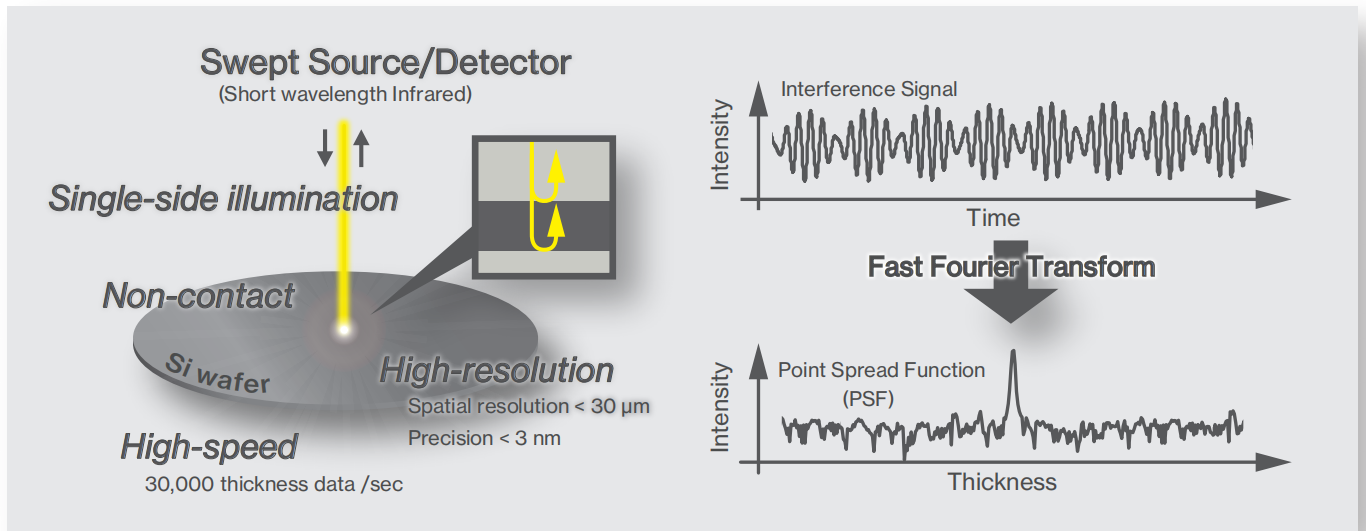
1. Flexible and applicable to more complex materials, from lightly doped to heavily doped P-type silicon (P++), silicon carbide, sapphire, glass, lithium niobate and other wafer materials.

Heavy doped silicon (front and rear surface detection of strongly absorbing wafers)
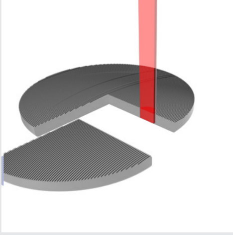
Rough wafer surface, (third-generation scanning frequency laser with point scanning, compared to spectral detection schemes, is less susceptible to interference noise from adjacent units in the spectrum, making it difficult to measure rough surface wafers)
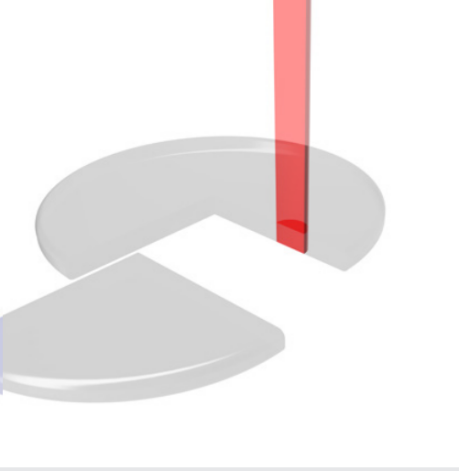
Low reflectivity silicon carbide (SiC) and lithium niobate (LiNbO3); (By compensating for polarization effects, enhance the signal-to-noise ratio of low reflection wafer surface measurements)

Silicon on insulator (SOI) and MEMS can simultaneously measure multi-layer structures, with thicknesses ranging from μ m to several hundred μ m.

It can be used to measure the thickness of various thin films, with the thinnest thickness as low as 4 μ m and an accuracy of up to 1nm.
1. The "temperature drift" processing capability of tunable swept frequency lasers is reflected in their strong anti-interference ability in extreme working environments, which changes the heavy reliance on "active damping platforms" in traditional wafer measurement and significantly reduces costs.
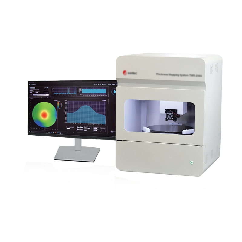
2. Flexible motion control method, compatible with measuring 2-inch to 12 inch square and circular pieces.