The methods for controlling the flatness of double-sided polishing of 12 inch recycled wafers mainly include the following:
1、 Adopting advanced polishing equipment and technology
Double sided polishing equipment:
Using double-sided polishing equipment to process wafers, this equipment can simultaneously control both sides of the workpiece, effectively avoiding deformation problems caused by stress differences and bonding errors.
Chemical mechanical polishing (CMP) technology:
CMP technology combines the dual effects of chemical corrosion and mechanical polishing, which can form a chemical reaction layer on the wafer surface and remove it through mechanical polishing, thereby achieving planarization of the wafer surface.
When using CMP technology, it is necessary to precisely control parameters such as the concentration, flow rate, pH value, and material of the polishing pad of the polishing solution to achieve the best polishing effect.
2、 Optimize polishing process parameters
Polishing time:
The length of polishing time directly affects the flatness of the wafer surface. It is necessary to set the polishing time reasonably based on the initial state and target flatness requirements of the wafer.
Pressure control:
The pressure between the wafer and polishing pad is one of the key factors affecting the polishing effect during the polishing process. Accurate control of polishing pressure is required to ensure consistent polishing rates throughout the wafer surface.
Rotation speed:
The rotation speed of the wafer and polishing pad during polishing can also affect the polishing effect. It is necessary to set the rotation speed reasonably to achieve a uniform polishing effect.
3、 Adopting unique processing techniques
Staged grinding:
Multiple grinding stages are used, such as coarse grinding, fine grinding, and polishing, to gradually remove the uneven parts of the wafer surface and ultimately achieve high flatness.
Special polishing solution:
Use specialized polishing solution, such as polishing powder containing specific particle sizes and concentrations, to optimize the polishing effect.
Polishing pad selection:
Choose suitable polishing pad materials, such as polyurethane polishing pads, and adjust the hardness and roughness of the polishing pad according to the polishing needs.
4、 Quality Control and Monitoring
Online monitoring:
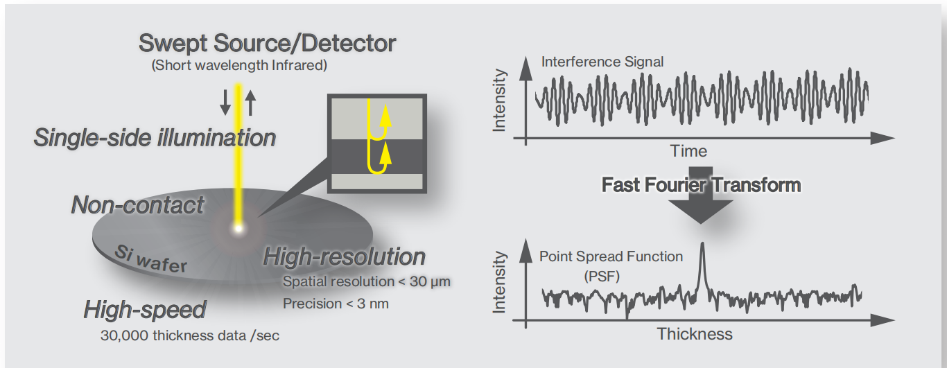
During the polishing process, a non-contact online measuring device is used to monitor the wafer thickness in real time to ensure the stability and accuracy of the polishing process.
Final inspection:
Strictly inspect and test the polished wafers, such as using scanning electron microscopy (SEM) or atomic force microscopy (AFM) to examine the surface morphology and roughness of the wafers, to ensure that their quality meets the requirements.
In summary, controlling the flatness of double-sided polishing of 12 inch recycled wafers requires comprehensive consideration of polishing equipment, polishing process parameters, processing technology, and quality control. By adopting advanced polishing equipment and technology, optimizing polishing process parameters, adopting unique processing techniques, and strengthening quality control and monitoring measures, the production of high flatness double-sided polished wafers can be achieved.
5、 High throughput wafer thickness measurement system
The high-throughput wafer thickness measurement system, based on the principle of optical coherence tomography, can solve technical indicators such as wafer/chip thickness TTV (Total Thickness Variation), BOW (Bend), WARP (Warpage), TIR (Total Marked Reading), STIR (Site Total Marked Reading), LTV (Local Thickness Variation), etc.
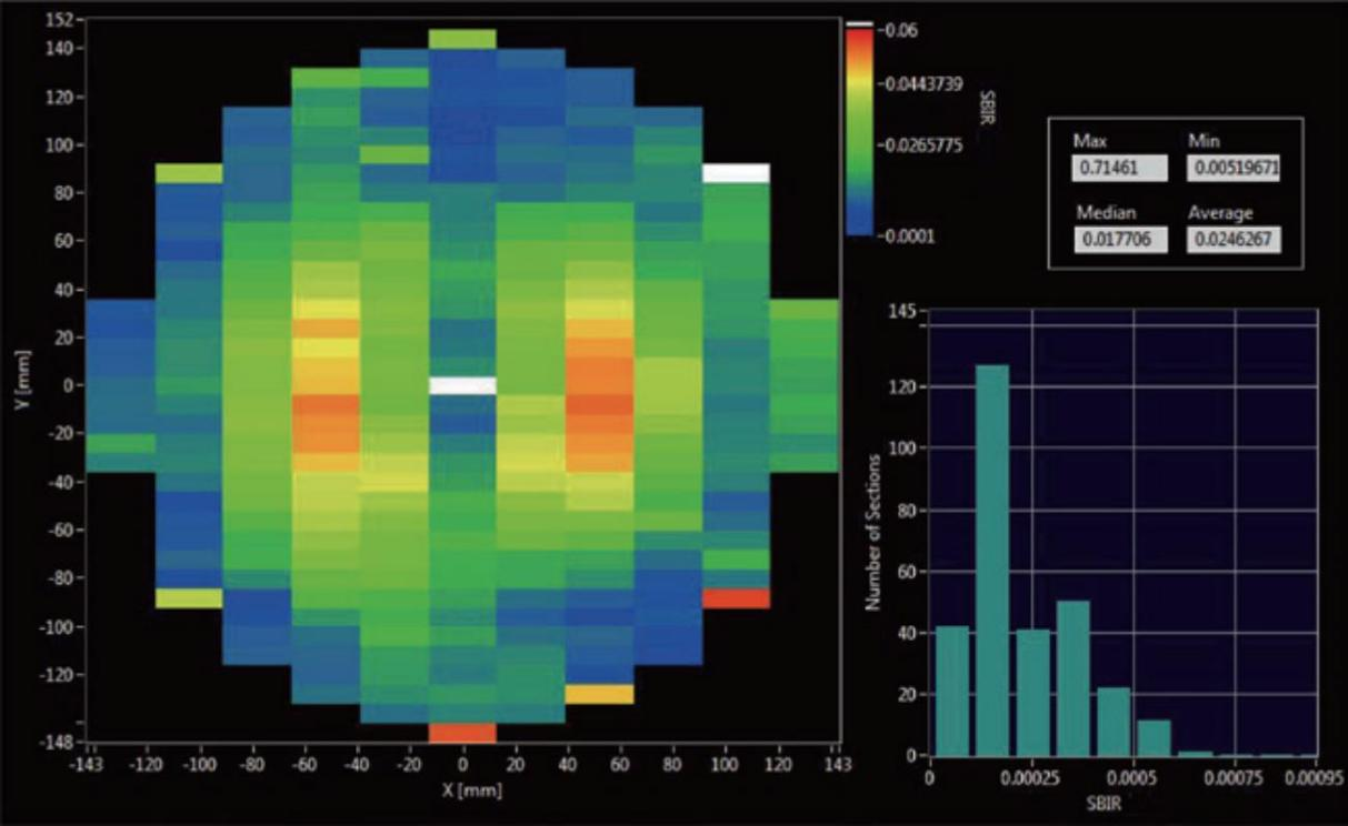
The high-throughput wafer thickness measurement system adopts the third-generation tunable scanning frequency laser technology, which is a traditional dual probe scanning method. It is compatible with 2-inch to 12 inch square and circular wafers, and can measure all flatness and thickness parameters at once.
1. Flexible and applicable to more complex materials, from lightly doped to heavily doped P-type silicon (P++), silicon carbide, sapphire, glass, lithium niobate and other wafer materials.

Heavy doped silicon (front and rear surface detection of strongly absorbing wafers)
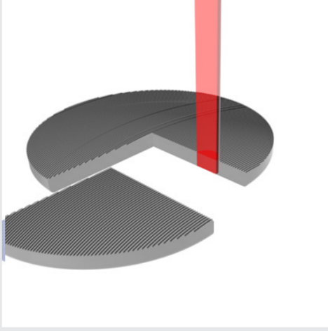
Rough wafer surface, (third-generation scanning frequency laser with point scanning, compared to spectral detection schemes, is less susceptible to interference noise from adjacent units in the spectrum, making it difficult to measure rough surface wafers)
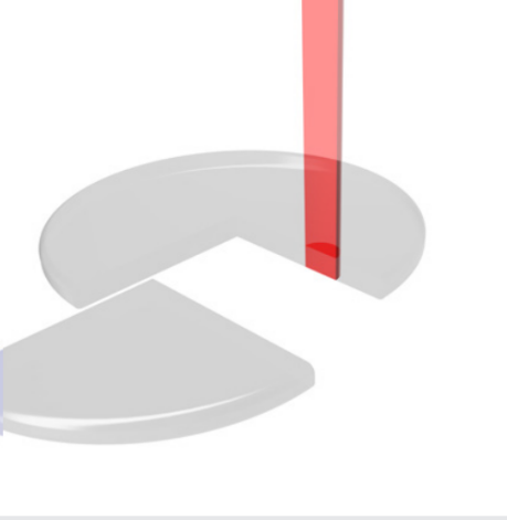
Low reflectivity silicon carbide (SiC) and lithium niobate (LiNbO3); (By compensating for polarization effects, enhance the signal-to-noise ratio of low reflection wafer surface measurements)
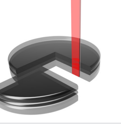
Silicon on insulator (SOI) and MEMS can simultaneously measure multi-layer structures, with thicknesses ranging from μ m to several hundred μ m.

It can be used to measure the thickness of various thin films, with the thinnest thickness as low as 4 μ m and an accuracy of up to 1nm.
1. The "temperature drift" processing capability of tunable swept frequency lasers is reflected in their strong anti-interference ability in extreme working environments, which changes the heavy reliance on "active damping platforms" in traditional wafer measurement and significantly reduces costs.
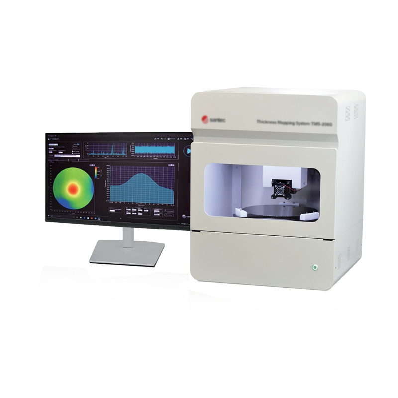
2. Flexible motion control method, compatible with measuring 2-inch to 12 inch square and circular pieces.