The device and method for single-sided polishing of wafers mainly involve the field of semiconductor equipment technology. The following is a detailed introduction to it:
1、 Single sided polishing device for wafers
The single-sided polishing device for wafers usually includes the following key components:
Workbench: As the foundation of the entire polishing device, it is used to support and fix other components. A servo motor is usually installed below the workbench to provide power during the polishing process.
Control electrical box: used to control various parameters and functions of the polishing device, ensuring the stability and accuracy of the polishing process.
Rotary table: placed on the slot of the workbench, with a fixed shaft connected below the rotary table. The servo motor rotates and is connected to the shaft to drive the rotary table to rotate. A polishing pad is installed above the turntable for contacting and polishing the wafer.
Polishing pad: Covering the turntable and in direct contact with the wafer, it plays a role in polishing and grinding. The material and hardness of the polishing pad have a significant impact on the polishing effect.
Wafer clamping device: used to fix the wafer to be polished, ensuring that the wafer will not move or fall off during the polishing process. The wafer clamping device is usually set on the polishing pad, leaving a certain gap between them, so that the polishing solution can be evenly distributed on the surface of the wafer.
Supporting device: set in the middle of the polishing pad, used to support the wafer and prevent it from deforming due to uneven force during the polishing process.
Polishing liquid spraying device: used to spray polishing liquid onto polishing pads and wafer surfaces to provide necessary polishing media and chemical reaction environment. The type and concentration of polishing solution have a significant impact on the polishing effect.
Rinsing device: used to rinse the wafer after polishing to remove polishing solution and impurities remaining on the surface of the wafer.
2、 Single sided polishing method for wafers
The single-sided polishing method for wafers usually includes the following steps:
Fixed wafer: Use a wafer clamping device to fix the wafer to be polished on the polishing pad, ensuring tight contact between the wafer and the polishing pad.
Spray polishing solution: Spray polishing solution evenly onto the polishing pad and wafer surface through a polishing solution spraying device. The type and concentration of polishing solution should be selected according to the wafer material and polishing requirements.
Start polishing: Start the servo motor to drive the turntable to rotate. Meanwhile, the wafer clamping device can rotate around its own axis to ensure uniform polishing of the wafer surface. During the polishing process, there is relative motion between the polishing pad and the wafer, and the abrasive particles and chemical components in the polishing solution work together to remove the uneven parts of the wafer surface.
Monitoring the polishing process: By monitoring the color differences on the polishing pad in real-time, the degree of polishing process can be determined. When the polishing meets the predetermined requirements, stop polishing.
Rinsing and drying: Use a rinsing device to rinse the polished wafer to remove residual polishing solution and impurities on the wafer surface. Then, the wafer is dried for use in subsequent processes.
In addition, there are other methods to improve the efficiency and quality of single-sided wafer polishing, such as using advanced polishing pad materials, optimizing polishing solution formulations, adjusting polishing parameters, etc. These methods can be selected and optimized based on specific needs and experimental conditions.
Overall, the single-sided polishing device and method for wafers are of great significance to the semiconductor manufacturing industry. By continuously improving and optimizing polishing equipment and methods, the polishing efficiency and quality of wafers can be improved, providing strong support for the manufacturing of semiconductor devices.
High throughput wafer thickness measurement system
The high-throughput wafer thickness measurement system, based on the principle of optical coherence tomography, can solve technical indicators such as wafer/chip thickness TTV (Total Thickness Variation), BOW (Bend), WARP (Warpage), TIR (Total Marked Reading), STIR (Site Total Marked Reading), LTV (Local Thickness Variation), etc.
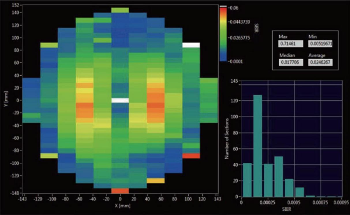
The high-throughput wafer thickness measurement system adopts the third-generation tunable scanning frequency laser technology, which is a traditional dual probe scanning method. It is compatible with 2-inch to 12 inch square and circular wafers, and can measure all flatness and thickness parameters at once.
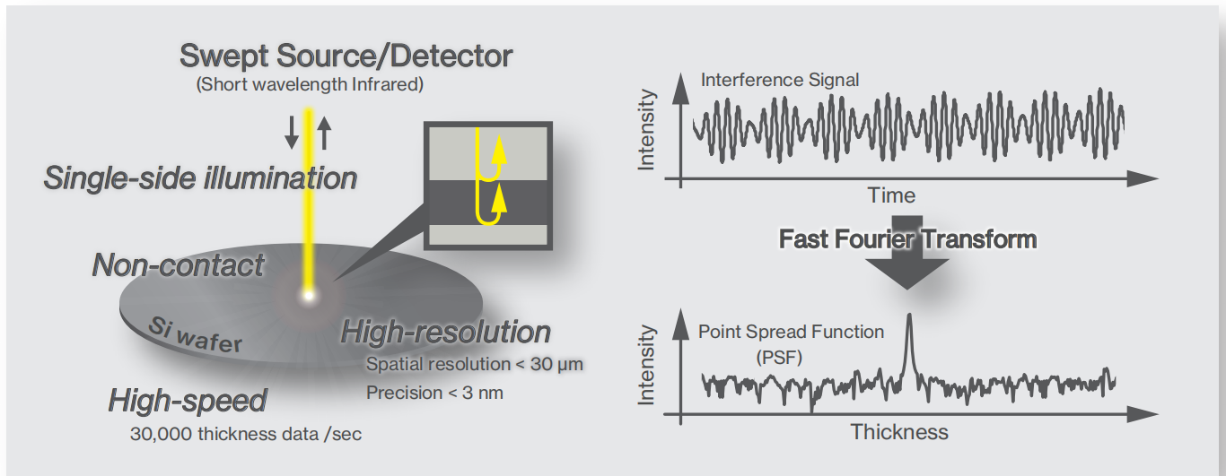
1. Flexible and applicable to more complex materials, from lightly doped to heavily doped P-type silicon (P++), silicon carbide, sapphire, glass, lithium niobate and other wafer materials.

Heavy doped silicon (front and rear surface detection of strongly absorbing wafers)
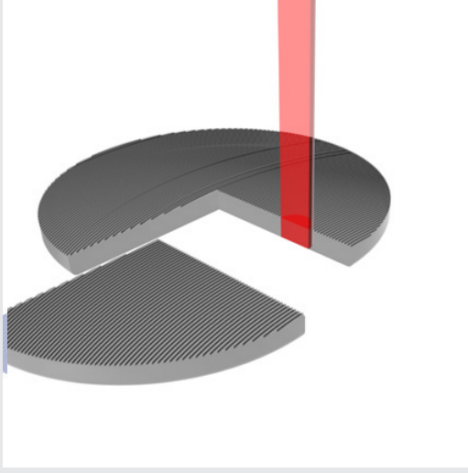
Rough wafer surface, (third-generation scanning frequency laser with point scanning, compared to spectral detection schemes, is less susceptible to interference noise from adjacent units in the spectrum, making it difficult to measure rough surface wafers)
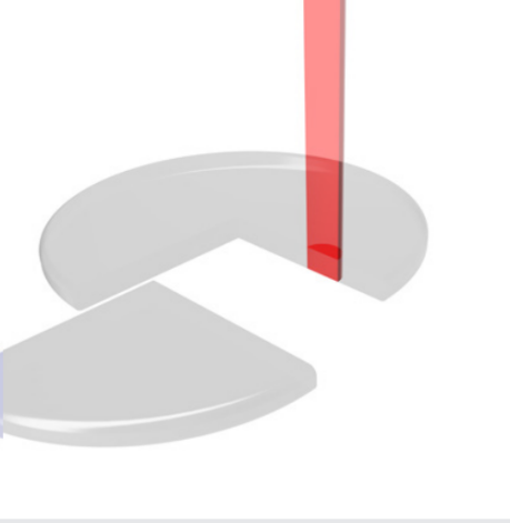
Low reflectivity silicon carbide (SiC) and lithium niobate (LiNbO3); (By compensating for polarization effects, enhance the signal-to-noise ratio of low reflection wafer surface measurements)
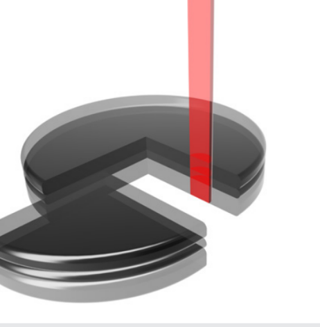
Silicon on insulator (SOI) and MEMS can simultaneously measure multi-layer structures, with thicknesses ranging from μ m to several hundred μ m.

It can be used to measure the thickness of various thin films, with the thinnest thickness as low as 4 μ m and an accuracy of up to 1nm.
1. The "temperature drift" processing capability of tunable swept frequency lasers is reflected in their strong anti-interference ability in extreme working environments, which changes the heavy reliance on "active damping platforms" in traditional wafer measurement and significantly reduces costs.
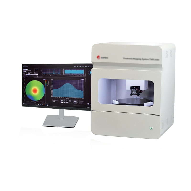
2. Flexible motion control method, compatible with measuring 2-inch to 12 inch square and circular pieces.